| CPC G09G 3/006 (2013.01) [H05K 3/42 (2013.01); H10K 59/131 (2023.02); G02F 1/133305 (2013.01)] | 14 Claims |
|
1. An electronic device comprising:
a display module defining a module hole that penetrates from the display module; and
an electronic module overlapping the module hole,
wherein the display module comprises:
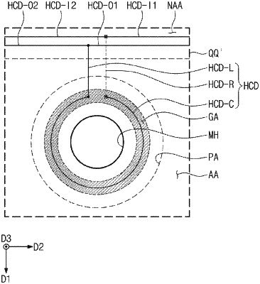
a display member divided into an active area, a peripheral area adjacent to the active area, and a hole area at least partially surrounded by the active area, and defining a groove overlapping the hole area and surrounding the module hole;
an input detection member disposed on the display member and including a detection insulating layer, and a first conductive pattern, and a second conductive pattern disposed on different layers with the detection insulating layer interpose therebetween; and
a crack detection wiring including a hole wiring overlapping the hole area, and a first detection wiring and a second detection wiring that are spaced apart from each other and extend from the hole area to the peripheral area to be connected to the hole wiring,
wherein the first detection wiring and the second detection wiring are disposed on different layers with the detection insulating layer interposed therebetween.
|