| CPC G06F 13/4282 (2013.01) [G06F 13/382 (2013.01); G06F 13/4004 (2013.01); G06F 2213/0016 (2013.01)] | 22 Claims |
|
1. A communication device comprising:
an I3C (Improved Integrated Circuit) device section that generates a command and data of I3C; and
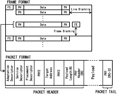
a communication device section including a first MIPI A-PHY circuit that transmits the command and data of the I3C to a second communication device including a second MIPI A-PHY circuit via a bus by using a payload in a protocol different from the I3C,
wherein the first MIPI A-PHY circuit receives the command and data of the I3C directly from the I3C device section,
wherein the I3C device section includes an I3C application program interface (I3C API) layer and an I3C link layer, the I3C API is configured to
convert first command and data of the I3C from a camera application program interface (camera API) into a first data format that is processable by the first MIPI A-PHY circuit, and
convert second command and data from the first MIPI A-PHY circuit into a second data format that is processable by the camera API,
wherein the I3C link layer is configured to
secure a physical communication with a communication partner, and
perform contention control, and
wherein the first MIPI A-PHY circuit receives the command and data of the I3C directly from the I3C link layer.
|