| CPC G06F 12/1081 (2013.01) [G06F 9/524 (2013.01); G06F 12/0246 (2013.01); G06F 12/0607 (2013.01); G06F 15/7807 (2013.01)] | 20 Claims |
|
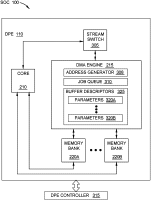
1. An integrated circuit (IC), comprising:
a switch;
a direct memory access (DMA) engine comprising multiple reconfigurable buffer descriptors configured with respective address generation parameters; and
a memory;
wherein the DMA engine is configured to:
receive data from the switch,
select a first one of the buffer descriptors for a first DMA write request based on a first instruction received by the DMA engine, and
write the data to the memory in a first non-sequential write pattern based on the address generation parameters of the first buffer descriptor.
|