| CPC G06F 11/1044 (2013.01) [G06F 9/30029 (2013.01); G06F 9/544 (2013.01); G06F 11/3037 (2013.01); G06F 12/0246 (2013.01); G11C 13/0004 (2013.01); G11C 13/004 (2013.01); G11C 13/0069 (2013.01)] | 9 Claims |
|
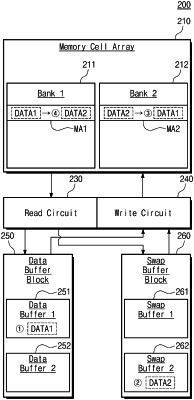
1. An operating method of a memory device comprising a memory cell array, a row decoder, a control circuit, a read circuit, a write circuit, a first buffer and a second buffer, the method executable by the control circuit and comprising operations of:
1) controlling the read circuit to read first data from a first location of the memory cell array identified by a first address;
2) controlling the first buffer to store the first data that is read in operation (1) or an error-corrected version of the first data;
3) controlling the write circuit to write the first data or the error-corrected version of the first data, which is stored in the first buffer, into a second location of the memory cell array identified by a second address;
4) controlling the second buffer to store second data written at the second location of the memory cell array or an error-corrected version of the second data; and
5) controlling the write circuit to write the second data or the error-corrected version of the second data, which is stored in the second buffer, into the first location of the memory cell array identified by the first address, wherein
operations (1) through (5) are performed in response to the control circuit receiving one or more commands from a memory controller that is disposed externally to the memory device.
|