| CPC G06F 3/0445 (2019.05) [G06F 3/044 (2013.01); G06F 3/0446 (2019.05); H01L 27/323 (2013.01); H01L 27/3253 (2013.01); H01L 51/5225 (2013.01); H01L 51/5246 (2013.01)] | 3 Claims |
|
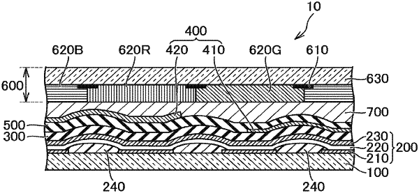
1. A semiconductor device comprising:
a first substrate having an insulating surface;
a circuit using thin film transistors on the insulating surface, the circuit comprises organic elements, each of the organic elements comprises a first electrode, a second electrode, and an organic layer between the first electrode and the second electrode;
a lower sealing layer on the circuit;
detection electrodes on the lower sealing layer;
an upper sealing layer covering the pair of detection electrodes; and
terminals around the circuit on the insulating surface, wherein
one of the detection electrodes is connected to one of the terminals via a contact hole formed in the lower sealing layer,
the detection electrodes comprise a first detection electrode layer and a second detection electrode layer,
a middle sealing layer is between the first detection electrode layer and the second detection electrode layer,
the first detection electrode layer is between the lower sealing layer and the middle sealing layer,
the second detection electrode layer is between the middle sealing layer and the upper sealing layer, and
at least one of the first detection electrode layer and the second detection electrode layer entirely covers the first electrode in a planar view.
|