| CPC G06F 3/044 (2013.01) | 10 Claims |
|
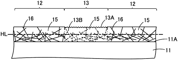
1. An electroconductive film comprising a light-transmitting base material, a plurality of light-transmitting electroconductive parts provided on one surface of the light-transmitting base material, and a light-transmitting nonconductive part located between the electroconductive parts,
wherein each of the electroconductive parts contains a light-transmitting resin and electroconductive fibers incorporated in the light-transmitting resin;
the nonconductive part contains a light-transmitting resin and exhibits no conductivity;
the three-dimensional arithmetic average roughness on a surface of the nonconductive part opposite the light transmitting base material is 6 nm or more and 80 nm or less; and
relative to a mid-point in the thickness direction of the electroconductive parts, the electroconductive fibers are unevenly distributed within the electroconductive parts such that there are more electroconductive fibers on the side facing the light-transmitting base material compared with the other side in the thickness direction.
|