| CPC G06F 3/0412 (2013.01) [G02F 1/13338 (2013.01); G02F 1/133305 (2013.01); G06F 3/0445 (2019.05); H01L 27/1214 (2013.01); H01L 27/323 (2013.01); H01L 27/3276 (2013.01); H01L 33/62 (2013.01); H01L 51/0097 (2013.01); G02F 1/13458 (2013.01); G02F 1/13629 (2021.01); G06F 2203/04103 (2013.01); H01L 2221/101 (2013.01); H01L 2224/83851 (2013.01); H01L 2227/326 (2013.01); H01L 2251/5338 (2013.01)] | 14 Claims |
|
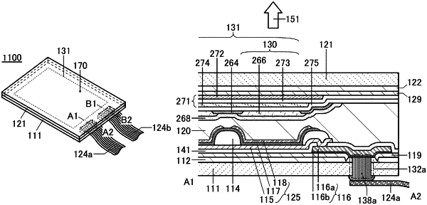
1. A display device comprising:
a first substrate;
a first insulating layer over the first substrate;
a transistor over the first insulating layer;
a first electrode configured to supply a first signal to the transistor;
a display element electrically connected to the transistor;
a second insulating layer over the display element;
a touch sensor over the second insulating layer;
a second electrode configured to supply a second signal to the touch sensor;
a second substrate overlapping with the first substrate; and
an external electrode under the first substrate,
wherein the first electrode is electrically connected to the external electrode through an opening,
wherein the second electrode is electrically connected to the external electrode through the opening,
wherein the opening is provided in the first substrate, the first insulating layer, and the second insulating layer, and
wherein the transistor comprises an oxide semiconductor material in a channel formation region.
|