| CPC G02F 1/1368 (2013.01) [G02F 1/137 (2013.01); G02F 1/1362 (2013.01); G02F 1/13439 (2013.01); G02F 1/13454 (2013.01); G02F 1/134309 (2013.01); G02F 1/134336 (2013.01); G02F 1/1339 (2013.01); G02F 1/13306 (2013.01); G02F 1/13394 (2013.01); G02F 1/13793 (2021.01); G02F 1/133302 (2021.01); G02F 1/133345 (2013.01); G02F 1/133357 (2021.01); G02F 1/133388 (2021.01); G02F 1/133512 (2013.01); G02F 1/133742 (2021.01); G02F 1/133784 (2013.01); G02F 1/136286 (2013.01); G02F 2201/121 (2013.01); G02F 2201/123 (2013.01)] | 19 Claims |
|
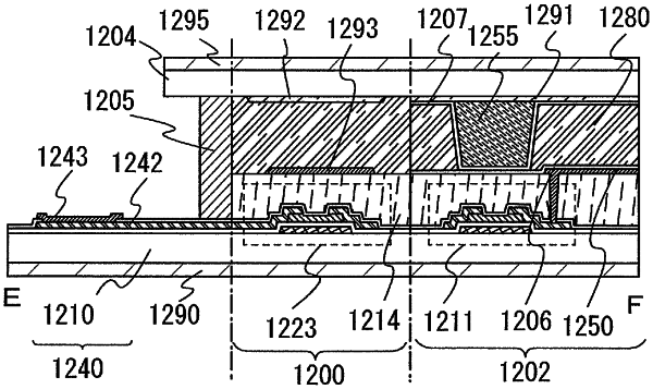
1. A semiconductor device comprising:
a first electrode layer and a second electrode layer over a first substrate;
a liquid crystal layer over the first electrode layer and the second electrode layer;
a first counter electrode layer and a second counter electrode layer over the liquid crystal layer;
a second substrate over the first counter electrode layer and the second counter electrode layer; and
a transistor in a driver circuit, the transistor comprising:
a channel formation region including an oxide semiconductor, the channel formation region comprising a first region; and
a source region including the oxide semiconductor, the source region comprising a second region,
wherein the first electrode layer is a pixel electrode formed in a position overlapping with the first counter electrode layer with the liquid crystal layer therebetween,
wherein the second electrode layer is an electrode layer of the driver circuit formed in a position overlapping with the second counter electrode layer with the liquid crystal layer therebetween,
wherein the first counter electrode layer and the second counter electrode layer do not overlap with each other,
wherein the first counter electrode and the second counter electrode are in contact with a same plane,
wherein the second counter electrode layer has a slit including a bend portion, and
wherein the second electrode layer is over the transistor and overlaps with the channel formation region of the transistor.
|