| CPC G02F 1/13629 (2021.01) [G02F 1/13439 (2013.01); G02F 1/13458 (2013.01); G02F 1/133345 (2013.01); G02F 1/134363 (2013.01); G02F 1/136227 (2013.01); G02F 1/136231 (2021.01); G02F 1/136295 (2021.01); G02F 1/1368 (2013.01)] | 15 Claims |
|
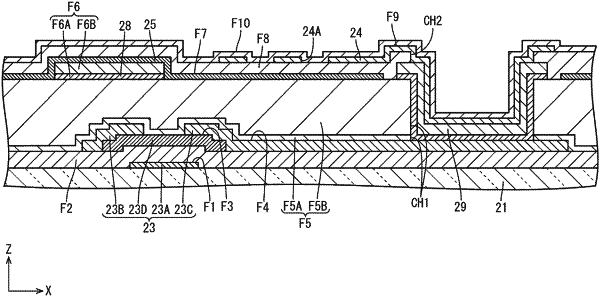
1. A display device comprising:
a switching element having a pixel connection portion;
a first insulating film, disposed at a higher layer than the pixel connection portion, that has a first pixel contact hole formed therein so as to be in a place overlapping at least a part of the pixel connection portion;
a common line disposed at a higher layer than the first insulating film;
an intermediate electrode composed of a conducting film which is identical to that of which the common line is composed, disposed to overlap the first pixel contact hole, and connected to the pixel connection portion;
a common electrode disposed at a higher layer than the common line, not connected to the intermediate electrode, and connected to the common line;
a second insulating film, disposed at a higher layer than the common electrode, that has a second pixel contact hole formed therein so as to be in a place overlapping at least a part of the intermediate electrode; and
a pixel electrode disposed at a higher layer than the second insulating film and disposed so that at least a part of the pixel electrode overlaps the second pixel contact hole.
|