| CPC G02F 1/136286 (2013.01) [G02F 1/136277 (2013.01)] | 20 Claims |
|
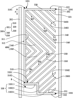
1. An array substrate, comprising a base substrate, a first electrode layer, an insulating dielectric layer, and a second electrode layer; wherein the array substrate further comprises a plurality of data leads; and one of the first electrode layer and the second electrode layer comprises at least one slit electrode;
the slit electrode is disposed between two adjacent data leads, and the slit electrode comprises an electrode connecting portion and a plurality of first strip-shaped sub-electrodes arranged in sequence, one end of each of the first strip-shaped sub-electrodes being connected to the electrode connecting portion;
the electrode connecting portion comprises a first connecting section parallel to and adjacent to the data lead, wherein the plurality of first strip-shaped sub-electrodes are disposed on a same side of the first connecting section; a width of the first strip-shaped sub-electrode gradually decreases along a direction going away from the first connecting section; and a distance between two adjacent first strip-shaped sub-electrodes in a direction parallel to an extending direction of the first connecting section gradually increases along the direction going away from the first connecting section;
the first connecting section has a first edge and a second edge which are opposite to each other and are parallel to the extending direction of the first connecting section; the second edge of the first connecting section is farther from the first strip-shaped sub-electrodes than the first edge of the first connecting section is;
in the plurality of first strip-shaped sub-electrodes connected to the first connecting section, a distance between first design reference points of any two adjacent first strip-shaped sub-electrodes is equal; and
wherein in one slit electrode, the first design reference point of the first strip-shaped sub-electrode is an intersection point of a first auxiliary design line of the first strip-shaped sub-electrode and an auxiliary design line of the first connecting section, the first auxiliary design line of the first strip-shaped sub-electrode is a straight line on which an orthographic projection of the first edge of the first strip-shaped sub-electrode on the base substrate is located, and the auxiliary design line of the first connecting section is a straight line on which an orthographic projection of the first edge of the first connecting section on the base substrate is located.
|