| CPC G02F 1/136222 (2021.01) [G02F 1/1368 (2013.01); G02F 1/136286 (2013.01); G02F 2201/123 (2013.01); G06F 3/0412 (2013.01)] | 11 Claims |
|
1. A liquid crystal display device comprising:
a first substrate;
a second substrate facing the first substrate;
a liquid crystal layer between the first substrate and the second substrate; and
a display region for providing images;
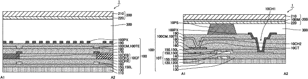
the first substrate comprising:
a thin-film transistor;
a pixel electrode connected to the thin-film transistor;
a color filter layer including color filters of multiple colors;
a touch panel line on a liquid crystal layer side of the color filter layer;
a flattening film on a liquid crystal layer side of the touch panel line; and
a plurality of touch panel electrodes arranged in a matrix on a liquid crystal layer side of the flattening film,
wherein the touch panel line is disposed at a boundary of the color filters of multiple colors of the color filter layer and connected to at least one of the plurality of touch panel electrodes in the display region,
the liquid crystal display device is provided with a first contact hole penetrating through at least the flattening film and a second contact hole penetrating through at least the flattening film,
the touch panel line is connected to the at least one of the plurality of touch panel electrodes through the second contact hole,
the color filter layer is not disposed in a continuous region including a region overlapping the first contact hole and a region overlapping a contact region where the touch panel line is in contact with the at least one of the plurality of touch panel electrodes, and
the pixel electrode is disposed on the liquid crystal layer side of the flattening film and is connected to a drain electrode of the thin-film transistor through the first contact hole.
|