US 11,668,982 B2
Liquid crystal display device
Yasushi Tomioka, Tokyo (JP); Yosuke Hyodo, Tokyo (JP); Hidehiro Sonoda, Tokyo (JP); and Noboru Kunimatsu, Tokyo (JP)
Assigned to Japan Display Inc., Tokyo (JP)
Filed by Japan Display Inc., Tokyo (JP)
Filed on Sep. 16, 2022, as Appl. No. 17/946,602.
Application 17/946,602 is a continuation of application No. 17/475,403, filed on Sep. 15, 2021, granted, now 11,480,833.
Application 17/475,403 is a continuation of application No. 16/953,997, filed on Nov. 20, 2020, granted, now 11,150,523, issued on Oct. 19, 2021.
Application 16/953,997 is a continuation of application No. 16/273,586, filed on Feb. 12, 2019, granted, now 10,877,325, issued on Dec. 29, 2020.
Application 16/273,586 is a continuation of application No. 16/158,402, filed on Oct. 12, 2018, granted, now 10,247,990, issued on Apr. 2, 2020.
Application 16/158,402 is a continuation of application No. 16/014,024, filed on Jun. 21, 2018, granted, now 10,126,611, issued on Nov. 13, 2018.
Application 16/014,024 is a continuation of application No. 15/891,707, filed on Feb. 8, 2018, granted, now 10,031,383, issued on Jul. 24, 2018.
Application 15/891,707 is a continuation of application No. 15/693,564, filed on Sep. 1, 2017, granted, now 9,921,440, issued on Mar. 20, 2018.
Application 15/693,564 is a continuation of application No. 15/401,795, filed on Jan. 9, 2017, granted, now 9,778,520, issued on Oct. 3, 2017.
Application 15/401,795 is a continuation of application No. 15/212,873, filed on Jul. 18, 2016, granted, now 9,575,385, issued on Feb. 21, 2017.
Application 15/212,873 is a continuation of application No. 14/978,671, filed on Dec. 22, 2015, granted, now 9,417,496, issued on Aug. 16, 2016.
Application 14/978,671 is a continuation of application No. 14/527,841, filed on Oct. 30, 2014, granted, now 9,250,491, issued on Feb. 2, 2016.
Claims priority of application No. 2013-226910 (JP), filed on Oct. 31, 2013.
Prior Publication US 2023/0020723 A1, Jan. 19, 2023
Int. Cl. G02F 1/13 (2006.01); G02F 1/1343 (2006.01); G02F 1/1362 (2006.01); G02F 1/1333 (2006.01); G02F 1/1335 (2006.01); G02F 1/1368 (2006.01); H01L 27/12 (2006.01); G02F 1/1337 (2006.01)
CPC G02F 1/134363 (2013.01) [G02F 1/1368 (2013.01); G02F 1/133345 (2013.01); G02F 1/133512 (2013.01); G02F 1/133514 (2013.01); G02F 1/133788 (2013.01); G02F 1/136227 (2013.01); H01L 27/1218 (2013.01); G02F 2202/02 (2013.01)] 14 Claims
OG exemplary drawing
 
1. A display device comprising:
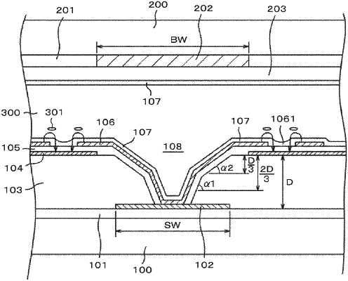
a first substrate including an organic passivation film, a common electrode formed on the organic passivation film, an insulating film on the common electrode, a pixel electrode on the insulating film, and a thin film transistor having a source electrode which is connected to the pixel electrode at a contact portion; and
a second substrate opposed to the first substrate, and including a black layer and a color filter on the second substrate,
wherein the organic passivation film around the contact portion has an inclined surface that is inclined with respect to the first substrate,
wherein the organic passivation film has a thickness D at a position opposed to the color filter, and
wherein an inclination angle of the inclined surface at a position of a thickness of D/3 is different from an inclination angle of the inclined surface at a position of a thickness of 2D/3.