| CPC G02B 6/305 (2013.01) | 7 Claims |
|
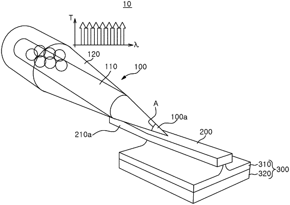
1. An interface for optical communication, comprising:
an input waveguide in which light input from an outside is guided;
an output waveguide including a first part abutting against one end of the input waveguide and a second part connected to the first part; and
a substrate including a Buried oxide (BOX) layer connected to a lower side of the output waveguide,
wherein the one end of the input waveguide includes a tapered structure of which a cross-sectional area is reduced by a predetermined angle,
wherein a width of the BOX layer is formed to be narrower than a width of the output waveguide.
|