| CPC G01T 1/245 (2013.01) [G01T 3/08 (2013.01); H01L 31/0322 (2013.01)] | 14 Claims |
|
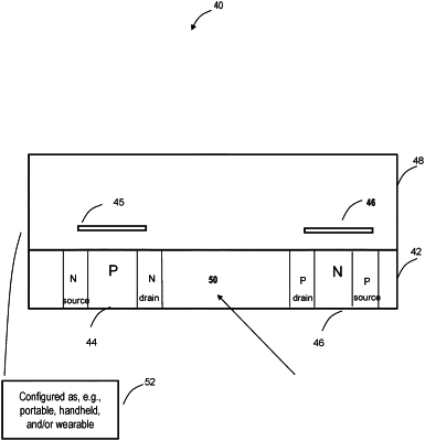
1. A wide band gap semiconductor NAND based neutron detection system comprising:
a single, active semiconductor layer as a wafer comprising a wide gap material with a neutron absorber material comprising at least one of lithium and boron in the wide band gap material, wherein the semiconductor layer is the only layer of the semiconductor NAND based neutron detection system fabricated with any neutron absorber material and located within the composition of the semiconductor layer;
wherein a memory structure is located within the wide band gap material and is configured to be cyclically read as a direct digital output by a controller.
|