| CPC G01R 31/54 (2020.01) [H03M 1/124 (2013.01)] | 20 Claims |
|
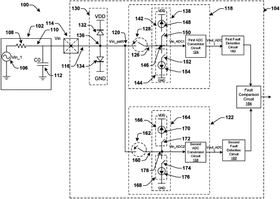
1. An analog fault detection circuit, comprising:
an input terminal configured to couple to an analog source circuit;
an input circuit path having a first end and a second end, and coupled to the input terminal at the first end; and
a first analog to digital converter (ADC) circuit comprising:
a first ADC conversion circuit configured to convert a first ADC input voltage to a first digital ADC output;
a first ADC circuit path coupled between the second end of the input circuit path and the first ADC conversion circuit, the first ADC circuit path comprising a first sampling switch, a first terminal of the first sampling switch is coupled to the second end of the input circuit path and wherein the first sampling switch is configured to sample an input path voltage at the second end of the input circuit path to provide the first ADC input voltage at a second terminal of the first sampling switch; and
a first broken wire detection circuit coupled between the first sampling switch and the first ADC conversion circuit, and configured to adaptively pulldown or pullup the first ADC input voltage, in order to detect a fault associated with a first analog circuit path, wherein the first analog circuit path includes the input circuit path and the first ADC circuit path;
a second ADC circuit comprising:
a second ADC conversion circuit configured to convert a second ADC input voltage to a second digital ADC output;
a second ADC circuit path coupled between the second end of the input circuit path and the second ADC conversion circuit, the second ADC circuit path comprising a second sampling switch, a first terminal of the second sampling switch is coupled to the second end of the input circuit path and wherein the second sampling switch is configured to sample the input path voltage at the second end of the input circuit path to provide the second ADC input voltage at a second terminal of the second sampling switch; and
a second broken wire detection circuit coupled between the second sampling switch and the second ADC conversion circuit, and configured to adaptively pulldown or pullup the second ADC input voltage, in order to detect a fault associated with a second analog circuit path, wherein the second analog circuit path includes the input circuit path and the second ADC circuit path.
|