| CPC G01R 31/31722 (2013.01) [G01R 31/2882 (2013.01); G01R 31/2886 (2013.01)] | 14 Claims |
|
1. An addressable test chip comprising:
a plurality of test pads;
a plurality of devices under test (DUTs); and
at least one peripheral circuit(s);
wherein:
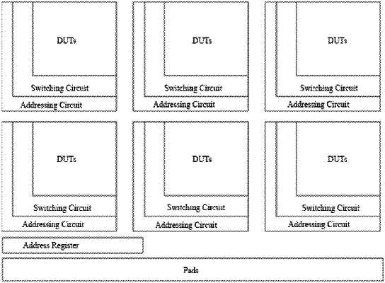
the DUTs are divided into at least one device array(s);
the peripheral circuit is configured to select several DUTs among the device array to be test through the on-state or off-state of the peripheral circuit units;
the peripheral circuit is designed according to the DUTs in the edge row or/and edge column of the device array, comprising: in the peripheral circuit area, configure the corresponding peripheral circuit unit for each DUT in the edge row or/and edge column of the device array, and place the peripheral circuit units, connect the DUTs of the device array and the corresponding peripheral circuit units through a wiring to form a peripheral circuit;
the peripheral circuit is designed according to the DUTs in the edge row or/and edge column of the device array, further comprising:
the row direction of an edge row or the column direction of the edge column is defined as X direction, and the peripheral circuit units to be placed meet the conditions comprising:
the first condition: the projection of the peripheral circuit unit and the projection of its corresponding DUT overlap in the X direction;
the second condition: there is no overlap in the X direction of the projection of peripheral circuit units in the same row or column;
the third condition: the peripheral circuit unit are placed within the peripheral circuit area.
|