| CPC G01R 31/2642 (2013.01) [G01R 31/2648 (2013.01); G01R 31/2831 (2013.01); G01R 31/2884 (2013.01); G01R 31/2886 (2013.01); H01L 22/34 (2013.01); H01L 2924/00 (2013.01); H01L 2924/0002 (2013.01)] | 20 Claims |
|
1. A method of analyzing defects in a semiconductor device, the method comprising:
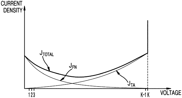
collecting current data by applying a test voltage to the semiconductor device;
extracting data within a decrease range from the current data;
dividing the current data into a first component value and a second component value using the current data and the data extracted from within the decrease range;
calculating a first quality index from the first component value satisfying a first function; and
calculating a second quality index from the second component value satisfying a second function that is different from the first function.
|