| CPC G01J 5/22 (2013.01) [G01J 5/0831 (2013.01); G01J 2005/202 (2013.01)] | 3 Claims |

|
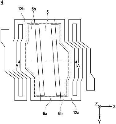
1. A thermistor element comprising:
a thermistor film;
a first electrode provided in contact with one surface of the thermistor film; and
a pair of second electrodes provided in contact with the other surface of the thermistor film, wherein
the thermistor film comprises an oxide having a spinel crystal structure and having a [111] preferred orientation in a film thickness direction, and
the [111] preferred orientation in a film thickness direction is:
a state in which a diffraction peak intensity from a (111) plane of the spinel crystal structure is greater than diffraction peak intensities from other crystal planes in a 0-20 scan by out-of-plane measurement of an X-ray diffraction method; or
a state in which only a diffraction peak from the (111) plane of the spinel crystal structure is observed in the 0-20 scan by the out-of-plane measurement of the X-ray diffraction method.
|