| CPC G01B 11/0633 (2013.01) [G01N 21/8422 (2013.01); G01N 21/9501 (2013.01); G06T 7/0004 (2013.01); G01N 2021/8427 (2013.01); G06T 2207/30148 (2013.01)] | 20 Claims |
|
1. A thickness estimation method comprising:
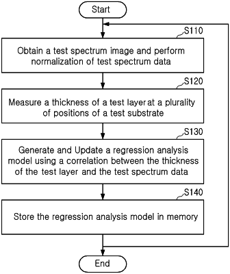
obtaining a test spectrum image from reflected light obtained by irradiating a test substrate with light;
obtaining test spectrum data included in a predetermined wavelength band at a plurality of positions on the test substrate, from the test spectrum image;
measuring a thickness of a test layer formed on the test substrate at the plurality of positions;
generating a regression analysis model using a correlation between the thickness of the test layer and the test spectrum data at the plurality of positions, and storing the regression analysis model in a memory;
irradiating a semiconductor substrate that is being transferred with light;
obtaining a spectrum image corresponding to an entire area of the semiconductor substrate; and
estimating a thickness of a target layer corresponding to the test layer over the entire area of the semiconductor substrate by applying the spectrum image to the regression analysis model.
|