US 11,667,126 B2
Printing material container, and board mounted on printing material container
Noboru Asauchi, Nagano (JP)
Assigned to SEIKO EPSON CORPORATION, Tokyo (JP)
Filed by SEIKO EPSON CORPORATION, Tokyo (JP)
Filed on Feb. 11, 2022, as Appl. No. 17/670,177.
Application 15/171,793 is a division of application No. 14/922,889, filed on Oct. 26, 2015, granted, now 9,381,750, issued on Jul. 5, 2016.
Application 17/670,177 is a continuation of application No. 17/036,780, filed on Sep. 29, 2020, granted, now 11,279,138.
Application 17/036,780 is a continuation of application No. 16/824,546, filed on Mar. 19, 2020, granted, now 10,836,173, issued on Nov. 17, 2020.
Application 16/824,546 is a continuation of application No. 16/289,094, filed on Feb. 28, 2019, granted, now 10,625,510, issued on Apr. 21, 2020.
Application 16/289,094 is a continuation of application No. 15/332,070, filed on Oct. 24, 2016, granted, now 10,259,230, issued on Apr. 16, 2019.
Application 15/332,070 is a continuation of application No. 15/171,793, filed on Jun. 2, 2016, granted, now 9,505,226, issued on Nov. 29, 2016.
Application 14/922,889 is a continuation of application No. 14/518,618, filed on Oct. 20, 2014, granted, now 9,180,675, issued on Nov. 10, 2015.
Application 14/518,618 is a continuation of application No. 14/332,973, filed on Jul. 16, 2014, granted, now 8,882,513, issued on Nov. 11, 2014.
Application 14/332,973 is a continuation of application No. 14/194,120, filed on Feb. 28, 2014, granted, now 8,801,163, issued on Feb. 28, 2014.
Application 14/194,120 is a continuation of application No. 13/902,171, filed on May 24, 2013, granted, now 8,794,749, issued on Aug. 5, 2014.
Application 13/902,171 is a continuation of application No. 13/608,658, filed on Sep. 10, 2012, granted, now 8,454,116, issued on Jun. 4, 2013.
Application 13/608,658 is a continuation of application No. 12/257,914, filed on Oct. 24, 2008, granted, now 8,366,233, issued on Feb. 5, 2013.
Application 12/257,914 is a continuation of application No. 12/040,308, filed on Feb. 29, 2008, granted, now 7,484,825, issued on Feb. 3, 2009.
Application 12/040,308 is a continuation of application No. 11/611,641, filed on Dec. 15, 2006, granted, now 7,562,958, issued on Jul. 21, 2009.
Claims priority of application No. 2005-372028 (JP), filed on Dec. 26, 2005; and application No. 2006-220751 (JP), filed on Aug. 11, 2006.
Prior Publication US 2022/0176705 A1, Jun. 9, 2022
This patent is subject to a terminal disclaimer.
Int. Cl. B41J 2/175 (2006.01); B41J 2/14 (2006.01)
CPC B41J 2/17526 (2013.01) [B41J 2/1752 (2013.01); B41J 2/1753 (2013.01); B41J 2/17503 (2013.01); B41J 2/17546 (2013.01); B41J 2/17566 (2013.01); B41J 2002/14491 (2013.01); B41J 2002/17579 (2013.01); Y10S 439/9241 (2013.01)] 9 Claims
OG exemplary drawing
 
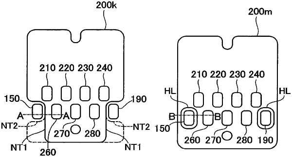
1. A circuit board mountable on a printing material container that is used in an ink jet printing apparatus, the ink jet printing apparatus having a print head and a plurality of apparatus-side contact forming members, the printing material container having a body and an ink supply opening, the ink supply opening having an exit on an exterior portion of the body and being adapted to supply ink from the printing material container to the printing apparatus, the circuit board comprising:
a memory device adapted to be driven by a memory driving voltage;
an electronic device adapted to receive a voltage higher than the memory driving voltage; and
a plurality of terminals having contact portions adapted and positioned to contact corresponding apparatus-side contact forming members so that electrical communication is enabled with the ink jet printing apparatus, the contact portions of the terminals including a plurality of memory contact portions electrically coupled to the memory device, a first electronic device contact portion electrically coupled to the electronic device, a second electronic device contact portion electrically coupled to the electronic device, and a short detection contact portion positioned and arranged to electrically contact a contact forming member that itself is electrically coupled to a short detection circuit of the printing apparatus, wherein:
the contact portions are arranged in a plurality of rows, and
the contact portions are arranged so that, the contact portion farthest to the left is the first electronic device contact portion, the contact portion that is farthest to the right is the second electronic device contact portion, the contact portion that is second farthest to the right is the short detection contact portion, and the memory contact portions are located to the left of the short detection contact portion and to the right of the first electronic device contact portion.