US 11,659,775 B2
Embedded MRAM fabrication process for ion beam etching with protection by top electrode spacer
Jun-Yao Chen, Hsinchu (TW); Harry-Hak-Lay Chuang, Hsinchu (TW); and Hung Cho Wang, Hsinchu (TW)
Assigned to Taiwan Semiconductor Manufacturing Co., Ltd., Hsinchu (TW)
Filed by Taiwan Semiconductor Manufacturing Co., Ltd., Hsinchu (TW)
Filed on Jun. 8, 2021, as Appl. No. 17/342,464.
Application 17/342,464 is a continuation of application No. 16/672,110, filed on Nov. 1, 2019, granted, now 11,063,208.
Claims priority of provisional application 62/868,637, filed on Jun. 28, 2019.
Prior Publication US 2021/0305496 A1, Sep. 30, 2021
Int. Cl. H01L 43/00 (2006.01); H01L 43/02 (2006.01); H01L 43/10 (2006.01); H01L 43/12 (2006.01)
CPC H01L 43/02 (2013.01) [H01L 43/10 (2013.01); H01L 43/12 (2013.01)] 20 Claims
OG exemplary drawing
 
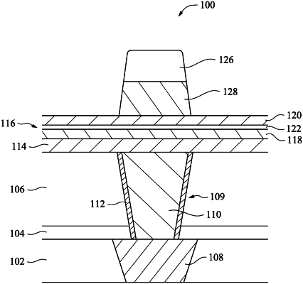
1. A structure, comprising:
a semiconductor substrate;
a first structure over the semiconductor substrate;
a first electrode positioned on a first surface of the first structure;
a first sidewall spacer positioned on the first surface of the first structure and laterally adjacent to a sidewall of the first electrode; and
a second sidewall spacer positioned laterally adjacent to a sidewall of the first structure and laterally adjacent to the first sidewall spacer.