| CPC H10N 50/01 (2023.02) [H01L 23/544 (2013.01); H10B 61/00 (2023.02); H10N 50/80 (2023.02); H01L 2223/54426 (2013.01)] | 10 Claims |
|
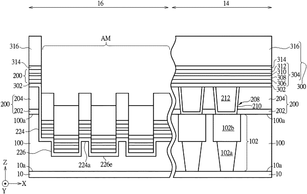
1. A method for forming a semiconductor structure, comprising:
providing a substrate having a device region and an alignment mark region;
forming a first dielectric layer on the substrate and a second dielectric layer on the first dielectric layer;
forming a conductive via in the second dielectric layer on the device region;
forming a mask layer on the second dielectric layer, the mask layer having an opening exposing the second dielectric layer on the alignment mark region;
performing a dry etching process through the opening to form a first trench and a plurality of second trenches directly under the first trench, wherein the first trench penetrates through the second dielectric layer and an upper portion of the first dielectric layer, the second trenches are completely in the first dielectric layer and exposed from a bottom surface of the first trench;
removing the mask layer; and
forming a memory stack structure on the second dielectric layer, wherein the memory stack structure completely covers a top surface of the conductive via and filling into the first trench and the second trenches.
|