| CPC H01L 27/3276 (2013.01) [H01L 27/3248 (2013.01); H01L 27/3262 (2013.01); H01L 27/1214 (2013.01)] | 20 Claims |
|
1. A display panel comprising:
a plurality of pixels comprising a first pixel and a second pixel, wherein the first pixel comprises a first light-emitting device and a first pixel circuit connected with each other, and the second pixel comprises a second light-emitting device and a second pixel circuit connected with each other;
a display area comprising an optical component area and a regular display area, wherein the first light-emitting device is arranged in the optical component area, and the second light-emitting device is arranged in the regular display area; and
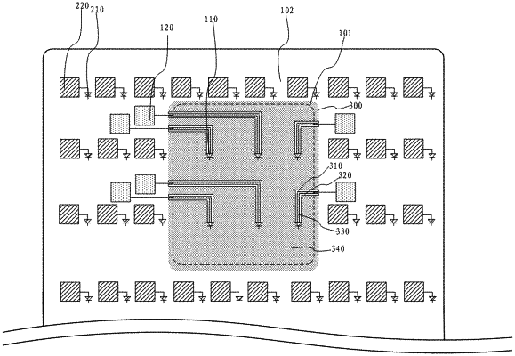
at least one transparent conductive layer arranged in the optical component area, wherein the transparent conductive layer comprises a first etching slot and a second etching slot that are paired with each other, a connection wire arranged between the first etching slot and the second etching slot that are paired with each other, and an auxiliary layer arranged outside the first etching slot and the second etching slot that are paired with each other;
wherein the display panel comprises a plurality of transparent conductive layers, and in a direction perpendicular to a plane on which the display panel is located, the first etching slot and/or the second etching slot of at least one of the transparent conductive layers is overlapped with the auxiliary layer of at least one of the other transparent conductive layers.
|