| CPC H10K 50/844 (2023.02) [H10K 71/00 (2023.02); H10K 71/70 (2023.02)] | 12 Claims |
|
1. An electronic device substrate, comprising:
a base substrate;
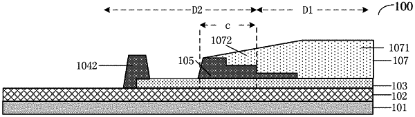
an organic encapsulation layer being on the base substrate and comprising a main part and an edge part; and
a padding structure being provided on the base substrate and protruding from the base substrate, wherein
the edge part of the organic encapsulation layer at least partially covers the padding structure; and a part that is comprised by the padding structure and is away from the main part of the organic encapsulation layer has a height with respect to the base substrate greater than a height of another part that is comprised by the padding structure and is close to the main part of the organic encapsulation layer with respect to the base substrate;
the electronic device substrate further comprises a barrier wall, the barrier wall is on the base substrate and on a side of the padding structure close to an edge of the base substrate, an interval is between the barrier wall and the padding structure, a height of the barrier wall with respect to the base substrate is greater than a height of the padding structure with respect to the base substrate, and the organic encapsulation layer does not cover the barrier wall;
a side of the padding structure away from the barrier wall has a step structure, the step structure includes multiple connected plane parts, top surfaces of the multiple plane parts are parallel to the base substrate; and in a direction toward the barrier wall, heights of the multiple plane parts of the step structure with respect to the base substrate gradually increase; and
a side of the padding structure facing the barrier wall is inclined with respect to the base substrate and is not step-like.
|