| CPC H01L 27/2436 (2013.01) [G11C 13/004 (2013.01); G11C 13/0069 (2013.01); H01L 27/1203 (2013.01); G11C 2213/74 (2013.01); G11C 2213/79 (2013.01)] | 22 Claims |
|
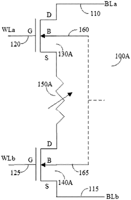
1. A resistive random-access memory (ReRAM) cell comprising:
a silicon over insulator (SOI) substrate;
a first metal-oxide semiconductor field-effect transistor (MOSFET) formed on the SOI substrate having a drain port, a gate port, a source port, and a bulk port;
a second MOSFET formed on the SOI substrate having a drain port, a gate port, a source port, and a bulk port;
a resistive element formed on the SOI substrate having a first port and a second port;
a word line connected to the gate port of the first MOSFET;
an inverted word line of the word line connected to the gate port of the second MOSFET;
a bit line; and
an inverted bit line of the bit line;
wherein the first MOSFET, the second MOSFET, and the resistive element are connected in series between the bit line and the inverted bit line;
wherein upon applying a predefined potential at the bit line, the inverted bit line, the word line, the inverted word line, the bulk port of the first MOSFET, and the bulk port of the second MOSFET, a state of the ReRAM cell is determined.
|