| CPC H01L 27/11597 (2013.01) [H01L 27/11502 (2013.01); H01L 27/11507 (2013.01); H01L 27/11587 (2013.01); H01L 27/11592 (2013.01); H01L 28/55 (2013.01); H01L 28/57 (2013.01); H01L 28/75 (2013.01)] | 19 Claims |
|
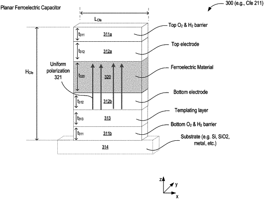
1. A ferroelectric device comprising:
a first layer comprising ferroelectric material;
a second layer over the first layer, the second layer comprising a metallic electrode;
a third layer under the first layer, the third layer comprising a metallic electrode; and
a fourth layer adjacent to the third layer, wherein the fourth layer is to induce crystallographic orientation in the first layer, and wherein the fourth layer comprises one of:
FePt with a lattice constant of about 3.86 Angstroms;
IrMn3 with a lattice constant of about 3.78 Angstroms;
Sr2RuO4 with a lattice constant of about 3.84 Angstroms; or
BiSrCaCuO with a lattice constant of about 3.83 Angstroms.
|