|
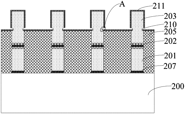
1. A fabrication method of a memory structure, comprising: providing a substrate; forming a plurality of discrete memory gate structures on the substrate, wherein an isolation trench is between adjacent memory gate structures, and a memory gate structure of the plurality of discrete memory gate structures includes a floating gate layer and a control gate layer on the floating gate layer; forming an isolation layer in the isolation trench, wherein a top surface of the isolation layer is lower than a top surface of the control gate layer and higher than a bottom surface of the control gate layer; forming an opening on an exposed sidewall of the control gate layer, wherein a bottom of the opening is lower than or coplanar with the top surface of the isolation layer; and forming an initial metal silicide layer on an exposed surface of the control gate layer and the top surface of the isolation layer.
|