| CPC H05K 1/0245 (2013.01) [H01P 1/20381 (2013.01); H01P 3/026 (2013.01); H05K 1/111 (2013.01); H05K 3/4644 (2013.01); H05K 2201/09236 (2013.01); H05K 2201/1006 (2013.01)] | 20 Claims |
|
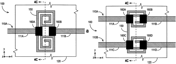
1. A printed circuit board, comprising:
a signal trace layer comprising:
a first signal trace comprising a first portion and a second portion, wherein the first and second portions of the first signal trace are disjoint,
a first component pad coupled to the first portion of the first signal trace,
a second component pad coupled to the second portion of the first signal trace,
a second signal trace, the second signal trace comprising a first portion and a second portion, wherein the first and second portions of the second signal trace are disjoint,
a third component pad coupled to the first portion of the second signal trace, and
a fourth component pad coupled to the second portion of the second signal trace; and
a reference plane situated under the signal trace layer, wherein the reference plane comprises a dual-spiral common-mode filter,
wherein:
a first at least part of the dual-spiral common-mode filter is situated under at least a portion of (a) the first component pad, (b) the second component pad, or (c) both (a) and (b),
a second at least part of the dual-spiral common-mode filter is situated under at least a portion of (i) the third component pad, (ii) the fourth component pad, or (iii) both (i) and (ii), and
the dual-spiral common-mode filter comprises a first spiral portion connected to a second spiral portion.
|