| CPC H04L 67/1097 (2013.01) [H04L 49/356 (2013.01); H04L 67/1095 (2013.01); H04L 67/61 (2022.05); H04L 2101/622 (2022.05)] | 19 Claims |
|
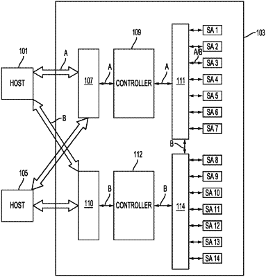
1. A Data Storage Device (DSD), comprising:
a plurality of solid-state memories for storing data;
one or more host network Ethernet switches configured to connect to one or more hosts;
at least one pair of storage area network Ethernet switches each configured to connect to one or more solid-state memories of the plurality of solid-state memories; and
a controller configured to:
receive a packet from a host via a host network Ethernet switch of the one or more host network Ethernet switches, the packet including a command to read or write data in a solid-state memory of the plurality of solid-state memories and a header to communicate between the host and the DSD;
change the header in the packet into an internal header to communicate between the controller and the solid-state memory; and
send, via a storage area network Ethernet switch of the at least one pair of storage area network Ethernet switches, an internal command and the internal header to the solid-state memory to perform the command.
|