| CPC H03F 3/217 (2013.01) [H03F 1/0205 (2013.01); H03F 1/565 (2013.01); H03F 3/2171 (2013.01); H03F 2200/171 (2013.01); H03F 2200/387 (2013.01); H03F 2200/451 (2013.01)] | 19 Claims |
|
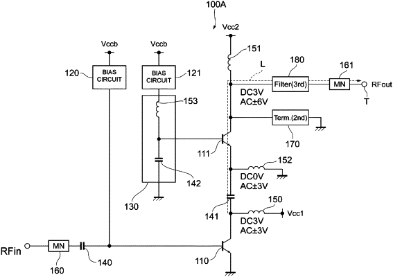
1. A power amplifier circuit comprising:
a lower transistor having a first terminal, a second terminal, and a third terminal, wherein a first power supply voltage is supplied to the first terminal, the second terminal is connected to ground, and an input signal is supplied to the third terminal;
a first capacitor;
an upper transistor having a first terminal, a second terminal, and a third terminal, wherein a second power supply voltage is supplied to the first terminal of the upper transistor, an amplified signal obtained by amplifying the input signal is output to an output terminal from the first terminal of the upper transistor, the second terminal of the upper transistor is connected to the first terminal of the lower transistor via the first capacitor, and a driving voltage is supplied to the third terminal of the upper transistor;
a first inductor that connects the second terminal of the upper transistor to ground; and
at least one termination circuit that short-circuits one of an even-order harmonic or an odd-order harmonic of the amplified signal to ground potential,
the at least one termination circuit being disposed so as to branch off from a node along a transmission path extending from the first terminal of the lower transistor to the output terminal through the first capacitor and the upper transistor.
|