| CPC H02M 3/07 (2013.01) [H02M 1/088 (2013.01)] | 31 Claims |
|
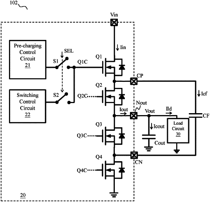
1. A switching capacitor power conversion circuit, comprising:
a conversion capacitor;
a plurality of conversion transistors, which are coupled to the conversion capacitor, wherein the plurality of conversion transistors are configured to operate so as to convert an input power to an output power at an output node; and
an output capacitor, which is coupled to the output node;
wherein in a switching conversion mode, the plurality of conversion transistors are configured to operably switch an electrical connection relationship of the conversion capacitor, such that the conversion capacitor is periodically electrically connected between one of at least one divided-voltage node and the input power, or between one of the at least one divided-voltage node and a ground level, or between a pair of the at least one divided-voltage node when the at least one divided-voltage node includes two or more divided-voltage nodes, thereby converting the input power to the output power, wherein the output node corresponds to a node of the at least one divided-voltage node, wherein in a steady state, a level of a voltage of the input power is k times of a level of a voltage of the output power, whereas, a level of a current of the input power is 1/k times of a level of a current of the output power, wherein k is a real number greater than one;
wherein in a pre-charging mode, the switching capacitor power conversion circuit is configured to operably perform following pre-charging operations, wherein:
during a first pre-charging period, the switching capacitor power conversion circuit is configured to operably control a first conversion transistor of the plurality of conversion transistors, so as to provide a first pre-charging current to pre-charge the conversion capacitor to a predetermined voltage level, wherein during the first pre-charging period, the first pre-charging current is prevented from charging the output capacitor; and
during a second pre-charging period, the switching capacitor power conversion circuit is configured to operably control a second conversion transistor of the plurality of conversion transistors, so as to provide a second pre-charging current via the output node to pre-charge the output capacitor to the predetermined voltage level, wherein during the second pre-charging period, the second pre-charging current is configured to operably supply a load current to a load circuit;
wherein the first pre-charging current is not greater than a first predetermined current level, whereas, the second pre-charging current is not greater than a second predetermined current level, and wherein the load current is not smaller than a third predetermined current level.
|