| CPC H01P 7/105 (2013.01) [H01P 1/15 (2013.01); H01P 1/20 (2013.01); H01P 1/2086 (2013.01); H01P 3/081 (2013.01); H05K 1/0237 (2013.01); H05K 1/14 (2013.01); H05K 9/0024 (2013.01); H04L 5/14 (2013.01)] | 10 Claims |
|
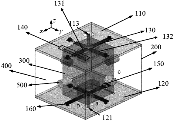
1. A dual-band filtering switch based on a single quad-mode dielectric resonator (DR), comprising:
a first printed circuit board (PCB) provided thereon with an input terminal;
a second PCB provided thereon with an output terminal, wherein the first PCB and the second PCB each comprise a respective feeding layer, a respective dielectric layer, and a respective ground layer that are stacked in sequence, the input terminal is electrically connected to the feeding layer of the first PCB, and the output terminal is electrically connected to the feeding layer of the second PCB;
a shielding shell arranged between the first and second PCBs and enclosing a shielding cavity together with the first and second PCBs; and
a single quad-mode DR arranged in the shielding cavity;
wherein the feeding layers of the first and second PCBs are both arranged facing the single quad-mode DR, and a respective feeding structure is formed on each of the respective feeding layers; the respective feeding structure comprises two perpendicularly intersecting microstrip lines, and the feeding structure is in contact with a respective surface of the single quad-mode DR; the first and second PCBs are each provided thereon with four short-circuited pins for connecting four ends of the microstrip lines to the respective ground layer; and
one end of each line of the two perpendicularly intersecting microstrip lines is respectively connected to a respective switching circuitry, and the switching circuitry is configured to control the dual-band filtering switch to be switched between an ON-state for dual-band transmission and an OFF-state for dual-band isolation.
|