| CPC H01L 33/62 (2013.01) [C25D 7/123 (2013.01); H01L 24/11 (2013.01); H01L 24/13 (2013.01); H01L 33/60 (2013.01); H01L 2224/1147 (2013.01); H01L 2224/11462 (2013.01); H01L 2224/13082 (2013.01); H01L 2224/13166 (2013.01); H01L 2224/13211 (2013.01); H01L 2224/13218 (2013.01); H01L 2224/13224 (2013.01); H01L 2224/13239 (2013.01); H01L 2224/13244 (2013.01); H01L 2224/13247 (2013.01); H01L 2224/13269 (2013.01); H01L 2924/0103 (2013.01); H01L 2924/014 (2013.01); H01L 2924/0105 (2013.01); H01L 2924/01013 (2013.01); H01L 2924/01029 (2013.01); H01L 2924/01047 (2013.01); H01L 2924/01078 (2013.01); H01L 2924/01079 (2013.01); H01L 2933/0058 (2013.01); H01L 2933/0066 (2013.01)] | 11 Claims |
|
1. A method for producing an optoelectronic component, the method comprising:
providing a semiconductor chip having an active region for radiation emission;
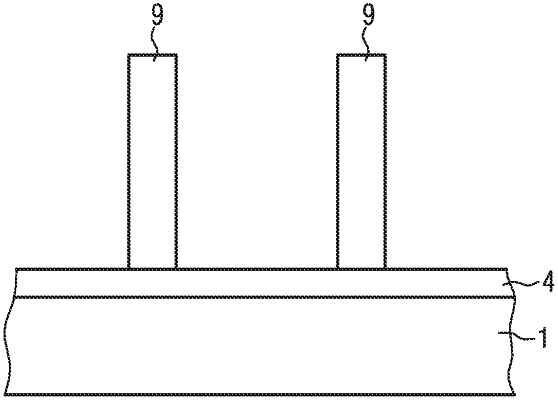
applying a seed layer on the semiconductor chip, wherein the seed layer comprises a first metal and a second metal being different from the first metal, and wherein the second metal is less noble than the first metal;
applying a structured photoresist layer directly to the seed layer; and
applying a solder layer at least to regions of the seed layer which are not covered by the photoresist layer,
wherein a proportion of the second metal in the seed layer is between 0.5 wt % and 10 wt %.
|