US 11,658,273 B2
Passivation for a semiconductor light emitting device
Frederic Stephane Diana, Santa Clara, CA (US); Kwong-Hin Henry Choy, Sunnyvale, CA (US); Qingwei Mo, Sunnyvale, CA (US); Serge L. Rudaz, Sunnyvale, CA (US); Frank L. Wei, San Francisco, CA (US); and Daniel A. Steigerwald, Cupertino, CA (US)
Assigned to Lumileds LLC, San Jose, CA (US)
Filed by LUMILEDS LLC, San Jose, CA (US)
Filed on Dec. 21, 2020, as Appl. No. 17/129,164.
Application 17/129,164 is a division of application No. 16/142,795, filed on Sep. 26, 2018, granted, now 10,873,013.
Application 15/077,620 is a division of application No. 13/904,299, filed on May 29, 2013, granted, now 10,134,964, issued on Nov. 20, 2018.
Application 16/142,795 is a continuation of application No. 15/077,620, filed on Mar. 22, 2016, granted, now 10,134,965, issued on Nov. 20, 2018.
Application 13/904,299 is a continuation of application No. 12/795,272, filed on Jun. 7, 2010, granted, now 8,471,282, issued on Jun. 25, 2013.
Prior Publication US 2021/0111321 A1, Apr. 15, 2021
This patent is subject to a terminal disclaimer.
Int. Cl. H01L 33/60 (2010.01); H01L 33/54 (2010.01); H01L 33/48 (2010.01); H01L 33/38 (2010.01); H01L 33/44 (2010.01); H01L 33/00 (2010.01); H01L 33/08 (2010.01); H01L 33/52 (2010.01); H01L 33/46 (2010.01); H01L 33/56 (2010.01)
CPC H01L 33/60 (2013.01) [H01L 33/0093 (2020.05); H01L 33/08 (2013.01); H01L 33/385 (2013.01); H01L 33/44 (2013.01); H01L 33/486 (2013.01); H01L 33/54 (2013.01); H01L 33/46 (2013.01); H01L 33/52 (2013.01); H01L 33/56 (2013.01); H01L 2933/005 (2013.01); H01L 2933/0025 (2013.01)] 20 Claims
OG exemplary drawing
 
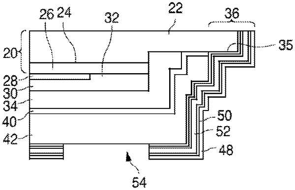
1. A method comprising:
providing a semiconductor structure comprising an active region between an n-type region and a p-type region, the semiconductor structure being divided into a plurality of light-emitting devices (LEDs) separated by a gap between adjacent LEDs of the plurality of LEDs;
removing a portion of the p-type region and the active region in the gap to form a first exposed surface region of the n-type region and in a region adjacent the gap to form a second exposed surface region;
disposing a dielectric layer at least directly on the first exposed surface region;
disposing an underfill in areas between the semiconductor structure and a mount at least directly on a portion of the dielectric layer and the second exposed surface region; and
attaching the semiconductor structure to the mount.