| CPC H01L 33/46 (2013.01) [H01L 33/382 (2013.01); H01L 33/38 (2013.01); H01L 33/405 (2013.01)] | 18 Claims |
|
1. A light-emitting device, comprising:
a semiconductor stack comprising a first semiconductor layer, a second semiconductor layer, and an active layer between the first semiconductor layer and the second semiconductor layer;
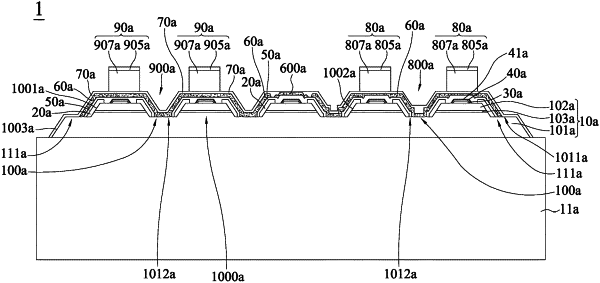
one or multiple vias penetrating the active layer and the second semiconductor layer to expose the first semiconductor layer;
a first contact layer covering the one or multiple vias;
a second contact layer on the second semiconductor layer, wherein the second contact layer does not overlap the first contact layer in a top view of the light-emitting device;
a second insulating layer comprising one or multiple second insulating openings to expose the first semiconductor layer, wherein the one or multiple second insulating openings are separated from each other and respectively corresponding to the one or multiple vias;
a third insulating layer comprising a first group of one or multiple third insulating openings formed on the second semiconductor layer to expose the first contact layer;
a first pad on the first contact layer and covering the first group of one or multiple third insulating openings; and
a second pad on the second contact layer, wherein in the top view of the light-emitting device, the second pad is separated from the first pad with a distance to define a region between the first pad and the second pad on the semiconductor stack, and the second pad is formed at a position other than positions of the one or multiple vias.
|