| CPC H01L 33/0095 (2013.01) [H01L 25/0753 (2013.01); H01L 2933/0066 (2013.01)] | 17 Claims |
|
1. A method for manufacturing a light emitting device, comprising:
providing a substrate with light emitting units disposed thereon;
attaching the light emitting units to a carrier;
removing the substrate; and
transferring a portion of the light emitting units from the carrier to a driving substrate, wherein transferring the portion of the light emitting units from the carrier to the driving substrate comprises:
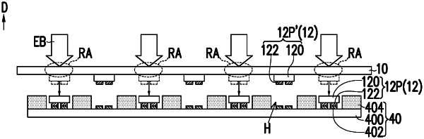
transferring the portion of the light emitting units from the carrier to another carrier, which comprises illuminating regions of the carrier overlapped with the portion of the light emitting units by an energy beam, wherein the other portion of the light emitting units is not transferred from the carrier to the another carrier; and
transferring the portion of the light emitting units from the another carrier to the driving substrate,
wherein a gap between the carrier and the another carrier when the carrier is illuminated by the energy beam is in a range from 1 μm to 300 μm, and the gap between the carrier and the another carrier is a distance between an outermost surface of the carrier facing the another carrier and an outermost surface of the another carrier facing the carrier along a stacking direction of the carrier and the another carrier.
|