| CPC H01L 31/173 (2013.01) [H01L 29/16 (2013.01); H01L 29/78 (2013.01); H01L 31/02019 (2013.01); H01L 31/02327 (2013.01); H01L 31/03044 (2013.01); H01L 31/1852 (2013.01); H01L 31/1856 (2013.01); H01L 33/007 (2013.01); H01L 33/32 (2013.01); H01L 33/60 (2013.01); H01L 2933/0058 (2013.01)] | 16 Claims |
|
1. A light source assembly comprising:
a plurality of cells, each of which including
a transistor including a drain region, and
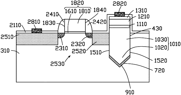
a light source comprising a first light source layer formed in a hole of a substrate, a light-generating layer, and a second light source layer, the first light source layer comprising a first sidewall and a second sidewall opposite to the first sidewall, wherein the drain region of the transistor is in contact with the first sidewall of the first light source layer and not in contact with the second sidewall of the first light source layer, and serves as a cathode of the light source; and
a driving circuit configured to drive each of the plurality of cells.
|