US 11,658,244 B2
Semiconductor device structure
Lin-Yu Huang, Hsinchu (TW); Jia-Chuan You, Dayuan Township, Taoyuan County (TW); Chia-Hao Chang, Hsinchu (TW); Tien-Lu Lin, Hsinchu (TW); Yu-Ming Lin, Hsinchu (TW); and Chih-Hao Wang, Hsinchu (TW)
Assigned to TAIWAN SEMICONDUCTOR MANUFACTURING COMPANY, LTD., Hsinchu (TW)
Filed by Taiwan Semiconductor Manufacturing Company, Ltd., Hsinchu (TW)
Filed on Jul. 19, 2021, as Appl. No. 17/379,446.
Application 17/379,446 is a division of application No. 16/548,423, filed on Aug. 22, 2019, granted, now 11,069,811.
Prior Publication US 2021/0351290 A1, Nov. 11, 2021
Int. Cl. H01L 29/78 (2006.01); H01L 29/66 (2006.01); H01L 21/308 (2006.01); H01L 21/768 (2006.01)
CPC H01L 29/785 (2013.01) [H01L 21/3081 (2013.01); H01L 21/3086 (2013.01); H01L 21/76816 (2013.01); H01L 21/76877 (2013.01); H01L 29/66795 (2013.01)] 20 Claims
OG exemplary drawing
 
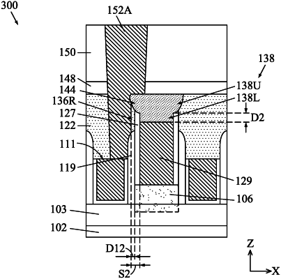
1. A semiconductor device structure, comprising:
a gate stack and a contact over a fin structure;
a gate spacer layer between the gate stack and the contact;
a first mask layer over the gate stack; and
a second mask layer over the contact, wherein the first mask layer includes a protruding portion sandwiched between an upper portion of the second mask layer and the gate spacer layer.