| CPC H01L 29/7816 (2013.01) [H01L 21/823481 (2013.01); H01L 29/0653 (2013.01); H01L 29/66681 (2013.01)] | 12 Claims |
|
1. A semiconductor device, comprising:
a substrate;
a first well region in the substrate, wherein the first well region has first ions;
an isolation layer in the first well region;
a second well region and a third well region, formed in the first well region, wherein the second well region and the third well region are respectively located on opposite sides of the isolation layer, the second well region and the third well region have second ions, the second ions and the first ions have opposite conductivity types, and a minimum distance of a distance between the second well region and the isolation layer, and a distance between the third well region and the isolation layer, is greater than zero;
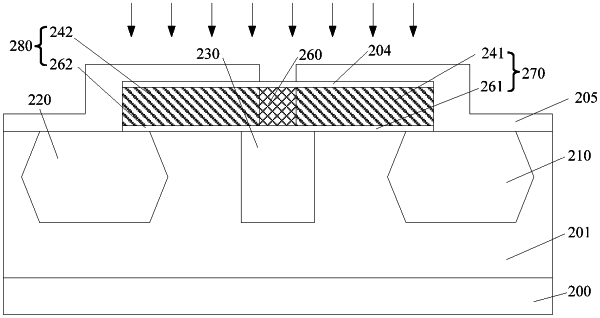
a first gate structure, on the second well region and the first well region;
a second gate structure, on the third well region and the first well region;
a third gate structure on the isolation layer, wherein the third gate structure is located between the first gate structure and the second gate structure, the first gate structure, the second gate structure, and the third gate structure are located over the substrate, and the third gate structure has the second ions; and
source-drain doped layers in the second well region and the third well region, respectively.
|