| CPC H01L 29/7786 (2013.01) [H01L 29/402 (2013.01); H01L 29/66462 (2013.01)] | 24 Claims |
|
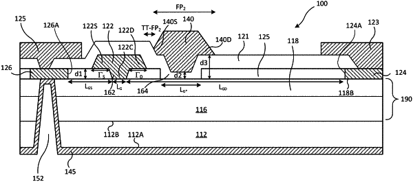
1. A transistor device, comprising:
a semiconductor epitaxial layer structure including a channel layer and a barrier layer on the channel layer, wherein the barrier layer has a higher bandgap than the channel layer;
a source contact and a drain contact on the barrier layer;
a first insulating layer on the barrier layer between the source contact and the drain contact; and
a gate contact on the first insulating layer, the gate contact comprising a central portion that extends through the first insulating layer and contacts the barrier layer, and a drain side wing that extends laterally from the central portion of the gate contact toward the drain contact by a distance GD, wherein the drain side wing of the gate contact is spaced apart from the barrier layer by a distance d1 that is equal to a thickness of the first insulating layer;
wherein the distance GD is less than about 0.3 μm; and
the distance d1 is less than about 80 nm;
wherein the transistor device exhibits an output power greater than 9 W/mm at an operating frequency of 10 GHz at a gate voltage of 50V while demonstrating a predicted lifetime greater than 106 hours at a junction temperature of 225 C.
|