| CPC H01L 29/7786 (2013.01) [H01L 21/0217 (2013.01); H01L 21/28581 (2013.01); H01L 21/28587 (2013.01); H01L 21/31111 (2013.01); H01L 21/765 (2013.01); H01L 29/2003 (2013.01); H01L 29/205 (2013.01); H01L 29/402 (2013.01); H01L 29/408 (2013.01); H01L 29/42316 (2013.01); H01L 29/475 (2013.01); H01L 29/66462 (2013.01); H03F 3/21 (2013.01); H03F 2200/451 (2013.01)] | 25 Claims |
|
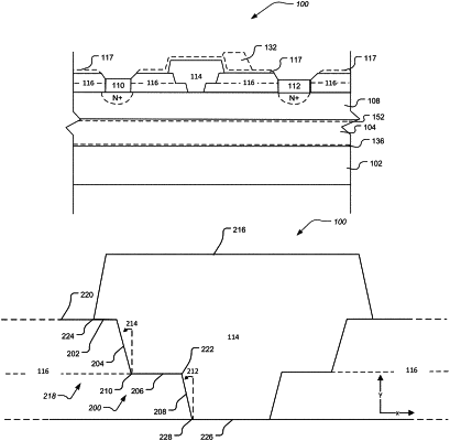
1. A device comprising:
a substrate;
a buffer layer on the substrate;
a barrier layer on the buffer layer;
a passivation layer on the barrier layer and the passivation layer comprising a recess;
a source electrically coupled to the barrier layer;
a gate on the barrier layer and the gate is structured and arranged to further extend across the passivation layer;
a drain electrically coupled to the barrier layer; and
the gate comprising at least one first surface connected to at least one second surface through at least one inflection point on either side of the recess,
wherein the at least one inflection point, the at least one first surface, and the at least one second surface are arranged within the passivation layer;
wherein the gate fills the recess of the passivation layer;
wherein the at least one first surface comprises at least four of the at least one first surface; and
wherein the at least one second surface comprises at least four of the at least one second surface.
|