US 11,658,226 B2
Backside gate contact
Huan-Chieh Su, Changua County (TW); Chun-Yuan Chen, HsinChu (TW); Li-Zhen Yu, Hsinchu (TW); Lin-Yu Huang, Hsinchu (TW); Lo-Heng Chang, Hsinchu (TW); Cheng-Chi Chuang, New Taipei (TW); and Chih-Hao Wang, Hsinchu County (TW)
Assigned to TAIWAN SEMICONDUCTOR MANUFACTURING COMPANY, LTD., Hsinchu (TW)
Filed by Taiwan Semiconductor Manufacturing Company, Ltd., Hsinchu (TW)
Filed on Apr. 13, 2021, as Appl. No. 17/228,955.
Claims priority of provisional application 63/151,228, filed on Feb. 19, 2021.
Prior Publication US 2022/0271138 A1, Aug. 25, 2022
Int. Cl. H01L 29/423 (2006.01); H01L 29/06 (2006.01); H01L 21/8234 (2006.01); H01L 29/786 (2006.01)
CPC H01L 29/42392 (2013.01) [H01L 21/823475 (2013.01); H01L 29/0665 (2013.01); H01L 29/42356 (2013.01); H01L 29/78696 (2013.01)] 20 Claims
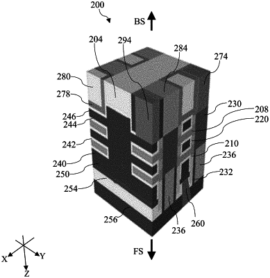
OG exemplary drawing
 
1. A semiconductor structure, comprising:
first nanostructures;
a first gate structure wrapping around each of the first nanostructures and disposed over an isolation structure;
a dielectric fin disposed on the isolation structure and in contact with a sidewall of the first gate structure; and
a backside gate contact disposed below the first nanostructures and adjacent to the isolation structure,
wherein a bottom surface of the first gate structure is in direct contact with the backside gate contact.