US 11,658,224 B2
Split gate memory device and method of fabricating the same
Chang-Ming Wu, New Taipei (TW); Wei Cheng Wu, Zhubei (TW); Shih-Chang Liu, Alian Township (TW); Harry-Hak-Lay Chuang, Zhubei (TW); and Chia-Shiung Tsai, Hsin-Chu (TW)
Assigned to Taiwan Semiconductor Manufacturing Company, Ltd., Hsinchu (TW)
Filed by Taiwan Semiconductor Manufacturing Company, Ltd., Hsin-Chu (TW)
Filed on Jun. 15, 2021, as Appl. No. 17/347,848.
Application 16/166,603 is a division of application No. 15/332,115, filed on Oct. 24, 2016, granted, now 10,147,794, issued on Dec. 4, 2018.
Application 17/347,848 is a continuation of application No. 16/705,508, filed on Dec. 6, 2019, granted, now 11,056,566.
Application 16/705,508 is a continuation of application No. 16/166,603, filed on Oct. 22, 2018, granted, now 10,516,026, issued on Dec. 24, 2019.
Application 15/332,115 is a continuation of application No. 14/182,952, filed on Feb. 18, 2014, granted, now 9,484,351, issued on Nov. 1, 2016.
Prior Publication US 2021/0313436 A1, Oct. 7, 2021
Int. Cl. H01L 29/423 (2006.01); H01L 27/11521 (2017.01); H01L 29/66 (2006.01); H01L 21/28 (2006.01); H01L 29/792 (2006.01); H01L 27/1157 (2017.01); H01L 27/11524 (2017.01); H01L 27/11568 (2017.01); H01L 29/51 (2006.01)
CPC H01L 29/42344 (2013.01) [H01L 27/1157 (2013.01); H01L 27/11521 (2013.01); H01L 27/11524 (2013.01); H01L 27/11568 (2013.01); H01L 29/40114 (2019.08); H01L 29/40117 (2019.08); H01L 29/42324 (2013.01); H01L 29/42348 (2013.01); H01L 29/518 (2013.01); H01L 29/6653 (2013.01); H01L 29/66825 (2013.01); H01L 29/66833 (2013.01); H01L 29/792 (2013.01)] 20 Claims
OG exemplary drawing
 
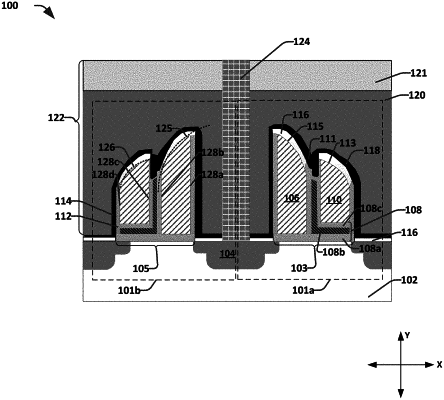
1. An integrated chip, comprising:
a source/drain region arranged within a substrate;
a first select gate arranged over the substrate;
a first memory gate arranged over the substrate and separated from the source/drain region by the first select gate; and
an inter-gate dielectric structure arranged between the first memory gate and the first select gate, the inter-gate dielectric structure extending under the first memory gate, wherein a height of a part of the inter-gate dielectric structure that is laterally between the first select gate and the first memory gate is smaller than a height of the first select gate.