| CPC H01L 29/4175 (2013.01) [H01L 29/0673 (2013.01); H01L 29/41725 (2013.01); H01L 29/42392 (2013.01); H01L 29/66439 (2013.01); H01L 29/66545 (2013.01); H01L 29/775 (2013.01); H01L 29/78696 (2013.01)] | 20 Claims |
|
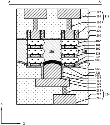
1. A semiconductor transistor device, comprising:
a channel structure;
a gate structure wrapping around the channel structure;
a first source/drain epitaxial structure and a second source/drain epitaxial structure disposed on opposite endings of the channel structure, the second source/drain epitaxial structure having a concave bottom surface; and
a back-side source/drain contact disposed under the first source/drain epitaxial structure; and
a first dielectric liner disposed along a sidewall of the back-side source/drain contact.
|