| CPC H01L 29/0634 (2013.01) [H01L 21/02532 (2013.01); H01L 21/02579 (2013.01); H01L 21/26513 (2013.01); H01L 21/3081 (2013.01); H01L 21/30604 (2013.01)] | 10 Claims |
|
1. A method for manufacturing a semiconductor super-junction device, comprising:
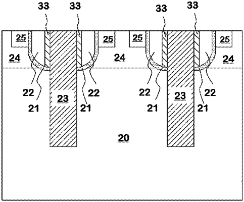
forming a hard mask layer on an n-type epitaxial layer, defining a position of a p-type column through a lithography process, etching the hard mask layer, and forming at least one opening in the hard mask layer, wherein the at least one opening corresponds to the position of the p-type column;
etching the n-type epitaxial layer with the hard mask layer as a mask, and forming a first trench in the n-type epitaxial layer, wherein a width of the first trench is larger than a width of one opening of the at least one opening corresponding to the first trench, and the first trench comprises a p-type column region located below the opening corresponding to the first trench and a gate region located on two sides of the p-type column region;
forming a first insulating layer on a surface of the first trench, depositing a first conductive layer and etching back the first conductive layer to form a gate in the gate region of the first trench;
forming an insulating side wall on an exposed side wall of the gate, etching the n-type epitaxial layer with the hard mask layer and the insulating side wall as masks, and forming a second trench in the n-type epitaxial layer, wherein the second trench is located below the p-type column region corresponding to the second trench; and
forming the p-type column in the p-type column region and the second trench, and forming a pn junction structure between the p-type column and the n-type epitaxial layer, wherein the p-type column is isolated from the gate by the insulating side wall.
|