| CPC H01L 27/14643 (2013.01) [H01L 27/14603 (2013.01); H01L 27/14609 (2013.01)] | 21 Claims |
|
1. A device, comprising:
a photodiode disposed in a semiconductor material, wherein the photodiode is coupled to generate charges in response to incident light;
a floating diffusion region disposed in the semiconductor material;
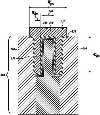
a transfer gate disposed between the photodiode and the floating diffusion region, wherein the transfer gate includes a plurality of fin structures that extend into the semiconductor material and the photodiode; and
a channel region associated with the transfer gate, disposed in the semiconductor material proximate to the transfer gate, wherein transfer gate is coupled to transfer the charges from the photodiode to the floating diffusion region through the channel region in response to a transfer signal coupled to be received by the transfer gate.
|