| CPC H01L 27/1463 (2013.01) [H01L 27/1464 (2013.01); H01L 27/14629 (2013.01); H01L 27/14612 (2013.01); H01L 27/14621 (2013.01); H01L 27/14627 (2013.01)] | 20 Claims |
|
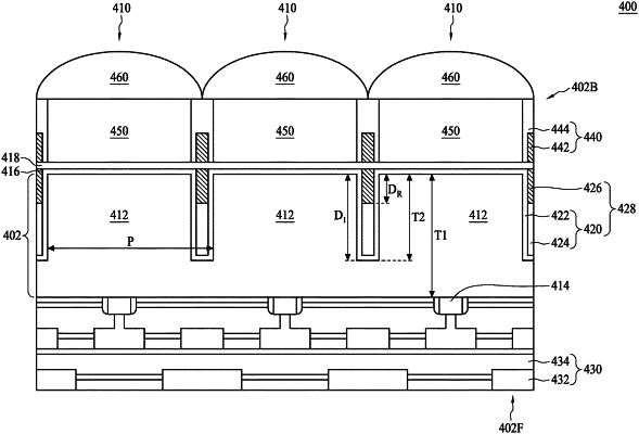
1. A back side illumination (BSI) image sensor comprising:
a substrate comprising a front side and a back side opposite to the front side;
a plurality of pixel sensors;
a first isolation grid disposed in the substrate and separating the plurality of pixel sensors from each other;
a first reflective grid disposed over the first isolation grid on the back side of the substrate;
a dielectric layer covering sidewalls of the first isolation grid and sidewalls of the first reflective grid;
a second isolation grid disposed over the back side of the substrate and overlapping the reflective grid from a plan view; and
a second reflective grid disposed between the second isolation grid and the substrate,
wherein a width of the second isolation grid is greater than a width of the first reflective grid.
|