| CPC H01L 27/1262 (2013.01) [H01L 27/124 (2013.01); H01L 27/1237 (2013.01); H01L 27/3244 (2013.01); H01L 25/167 (2013.01); H01L 27/1248 (2013.01); H01L 27/15 (2013.01)] | 16 Claims |
|
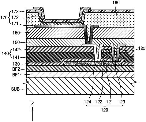
1. A display apparatus comprising:
a substrate;
a first buffer layer disposed on the substrate, the first buffer layer including silicon nitride and having an atomic percentage of hydrogen bonded to silicon of greater than 0.36 and equal to or less than 1.01;
a thin film transistor disposed over the first buffer layer; and
a display element electrically connected to the thin film transistor,
wherein the thin film transistor comprises a gate electrode and an active layer and the active layer is closer to the first buffer laver than the gate electrode is to the first buffer layer, and
wherein the gate electrode includes a first laver including aluminum, and a second layer disposed on the first layer, the second layer including a material having an etch ratio that is smaller than an etch ratio of aluminum.
|