| CPC H01L 27/0285 (2013.01) [H01L 27/0218 (2013.01); H01L 29/0619 (2013.01); H01L 29/0649 (2013.01)] | 9 Claims |
|
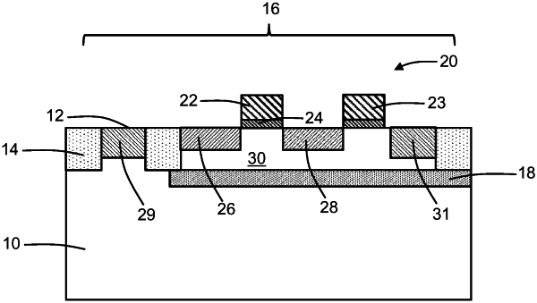
1. A structure comprising:
a bulk semiconductor substrate including a device region;
a substrate contact coupled to a portion of the bulk semiconductor substrate in the device region, the substrate contact configured to be biased with a first negative bias voltage;
a field-effect transistor including a semiconductor body in the device region of the bulk semiconductor substrate, the semiconductor body electrically isolated from the portion of the bulk semiconductor substrate; and
an isolation layer positioned between the semiconductor body and the portion of the bulk semiconductor substrate, the isolation layer comprising a polycrystalline semiconductor material.
|