| CPC H01L 25/18 (2013.01) [H01L 21/56 (2013.01); H01L 23/041 (2013.01); H01L 23/3121 (2013.01); H01L 24/32 (2013.01); H01L 24/33 (2013.01); H01L 24/48 (2013.01); H01L 2224/32059 (2013.01); H01L 2224/32145 (2013.01); H01L 2224/3303 (2013.01); H01L 2224/33051 (2013.01); H01L 2224/48221 (2013.01)] | 13 Claims |
|
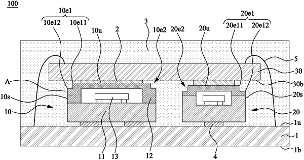
1. A semiconductor package structure, comprising:
a substrate;
a first electronic component disposed on the substrate, wherein the first electronic component has an upper surface and a lateral surface and a first edge between the upper surface and the lateral surface;
an interlayer on the upper surface of the first electronic component;
a third electronic component attached to the upper surface of the first electronic component via the interlayer; and
an encapsulant encapsulating the first electronic component and the interlayer;
wherein the interlayer does not contact the lateral surface of the first electronic component,
wherein the first edge of the first electronic component is a first recessed edge.
|